As a highly technical collection of multiple processes, each with a large number of steps, semiconductor manufacturing is a fertile ground for applying Lean and Six Sigma methodologies to reduce defects, improve flow, reduce wastes, and optimize processes. We’ll look at the successful applications in three case studies and finish with a video of how microchips are made.
Applying DMAIC Methodology to Address Probe Yield Issues
In a peer-reviewed book chapter titled “Application of Six Sigma in Semiconductor Manufacturing: A Case Study in Yield Improvement,” author Prashant Reddy Gangidi presents a comprehensive case study where Six Sigma DMAIC methodology was used to address a probe yield issue due to in-line defect contamination occurring in a lithography process step.
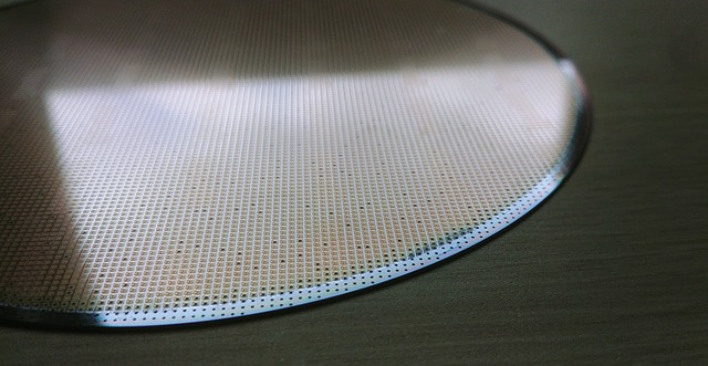
Problem Statement: Defects occur on about 25% of wafers around the edge resulting in bin failure and die loss on specific technology nodes.
See Table 1 in the chapter for the Project Charter. The project aim was to reduce die yield loss to ~1–2% from 7% by reducing in-line defects.
The case study pointed to the lithography process. During the Analyze phase, the team used a cause and effect diagram to list the potential causes. Table 2 in the study shows the various tools used to develop a validation plan for the various causes.
Further statistical analysis focused the attention on three tools used in the specific process and highlighted tool 1 as the potential contributor to the defect occurrence.
The design of experiments was used in the Improve phase to determine optimal tool settings.
In the Control phase, the team conducted a process FMEA to determine corrective actions for the Control Plan.
You can access this excellent case study at the following link.
[NOTE: Required Citation for Chapter
Prashant Reddy Gangidi (January 3rd 2019). Application of Six Sigma in Semiconductor Manufacturing: A Case Study in Yield Improvement, Applications of Design for Manufacturing and Assembly, Ancuţa Păcurar, IntechOpen, DOI: 10.5772/intechopen.81058. Available from: https://www.intechopen.com/chapters/64172]
Using Six Sigma to Reduce Electrical Failure Defects: Mexico
In a case study titled “Implementation of Six Sigma in a Manufacturing Process: A Case Study,”
authors Adan Valles, Jaime Sanchez, Salvador Noriega, and Berenice Gómez Nuñez discuss the application of Six Sigma to reduce the defects found in inkjet printer circuit cartridges during the electrical tests.
Before implementing the project, electrical failures accounted for about 50% of all defects.
In the Define phase, the critical characteristic was determined as the internal electrical defects detected during the electrical test.
During the Measure phase, the validity of the measurement system was studied.
In the Analyze phase the tools used to highlight potential causes were brainstorming, Pareto analysis, and cause and effect matrix. Statistical analysis was then used to test hypotheses about the main defect causes.
Further analysis focused on shift differences among the four shifts A through D. Shift A was found to have the best electrical test performance with lower defects and less variation than the other three.
During the Improve phase, once the factors that significantly affected the response variable were identified, possible improvement solutions were determined, implemented, and the improvement achieved was verified to be similar to that expected from experimental designs.
In the Control phase, an action plan was put in place to achieve a reduction in electrical failures.
Initially, the base defect percentage was 3.2%. After the project, it was 1.32%
You can read this excellent case study at the following link.
Lean and Six Sigma Applied to the Bill of Materials (BOM) Formatting Process: Malaysia
In a case, study titled “Improvement on Bill of Materials Formatting Process by Adopting Lean and Six Sigma Approaches A Case Study in a Semiconductor Industry,” authors Ilhammee Abd Wahab and others discuss the successful application of Lean and Six Sigma to reducing Bill of Materials processing time and the elimination of waiting and motion wastes.
BOM formatting is the main prerequisite for products assembly activities in manufacturing.
The project case study includes
- Project Charter
- Voice of Customers Summary
- Current State Mapping
- Ishikawa Diagram (Root Cause Analysis)
- 5 Whys Analysis
- Solution Concept Brainstorm Summary
- Macro Graphic Design and Design Flow
- Future State Mapping
Standard operating procedure for BOM was developed in the Control phase and training given to the relevant BOM workers.
As a result of the project, the company reduced the BOM processing time from an average of 50 minutes to five minutes. Manual touches went from 290 to 30 touches. Waiting time and motion waste elimination contributed to a financial savings of $1680 per month.
You can read the case study here.
[NOTE: Be patient. It’s a little slow to load.]
Video on How Microchips are Made
Watch an interesting video from Infineon Technologies AG on the chip-making process from silicon sand to the final product.
You can watch the video at this link.
Interested in expanding your knowledge on Lean Six Sigma? Take your career to the next level and join ISSSP today! Access the hundreds of videos, webinars, whitepapers, case studies, and other resources available in our library.


Leave A Comment